
TL;DR
Intel has commenced shipping silicon wafers manufactured using high-NA EUV lithography. This development signifies progress in next-generation semiconductor fabrication, though full production details remain undisclosed.
Intel has started shipping silicon wafers fabricated using high-NA EUV (extreme ultraviolet) lithography technology, marking a major milestone in the company’s advanced manufacturing capabilities. This development is significant because high-NA EUV is expected to enable smaller, more powerful chips, and Intel’s move indicates progress toward commercial adoption of this technology.
According to Intel, the company has begun delivering silicon wafers created with high-NA EUV lithography equipment from ASML, a key supplier of advanced lithography tools. This marks the first known instance of high-NA EUV being used in production at scale, moving beyond pilot or R&D phases. Intel’s announcement suggests that the company is actively integrating this technology into its manufacturing process, aiming to improve chip density and performance. High-NA EUV differs from standard EUV by utilizing a higher numerical aperture, which allows for finer feature sizes on chips. While Intel has not disclosed specific production volumes or timelines, sources close to the company indicate that this step is part of its broader roadmap to transition to more advanced nodes in the next few years. The shipping of wafers with high-NA EUV also underscores Intel’s efforts to stay competitive with other chipmakers investing in similar technology, such as TSMC and Samsung.Why Shipping High-NA EUV Silicon Is a Major Industry Milestone
This development is important because high-NA EUV lithography is considered a critical enabler for the next generation of semiconductor nodes, potentially allowing for smaller, faster, and more energy-efficient chips. Intel’s move to ship wafers using this technology indicates that it is progressing toward commercialization, which could influence industry standards and supply chain dynamics. For consumers and device makers, this could translate into more advanced processors and integrated circuits in the coming years. However, it remains to be seen how quickly Intel will scale production and how this will impact the broader chip market.
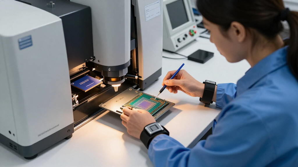
EUV lithography semiconductor equipment
As an affiliate, we earn on qualifying purchases.
As an affiliate, we earn on qualifying purchases.
Background on EUV and High-NA Lithography in Semiconductor Manufacturing
Extreme ultraviolet (EUV) lithography has been a key focus for advancing chip manufacturing beyond the 7nm node. Standard EUV tools, introduced by ASML, have been used in production since around 2019, enabling smaller feature sizes. High-NA EUV, an evolution of this technology, offers a higher numerical aperture, which is essential for further shrinking features below 3nm. While ASML began shipping high-NA EUV tools in limited quantities in recent years, commercial deployment at scale by chipmakers has been anticipated but not confirmed until now. Intel’s announcement aligns with industry expectations that high-NA EUV would eventually become a standard part of advanced manufacturing processes.
“We are pleased to announce that Intel has begun shipping silicon wafers produced with high-NA EUV technology, marking a significant step forward in our manufacturing roadmap.”
— Intel spokesperson
Details on Production Volume and Timeline Still Unclear
While Intel has confirmed the shipping of wafers produced with high-NA EUV, it is not yet clear how extensive this production is or when it will become a standard process for all manufacturing nodes. Specific timelines, production volume figures, and how quickly Intel plans to scale this technology remain undisclosed. Additionally, the full impact on product performance and cost is still uncertain as the technology transitions from early deployment to mainstream manufacturing.
Next Steps Include Scaling and Validation of High-NA EUV Production
Intel is expected to continue refining its high-NA EUV process, with plans to increase wafer volume and improve yield. Industry analysts anticipate that further validation and testing will precede broader adoption across more advanced nodes. The company may also collaborate with ASML to optimize equipment and process parameters. Monitoring Intel’s upcoming quarterly reports and industry announcements will provide more clarity on the pace of adoption and impact.
Key Questions
What is high-NA EUV lithography?
High-NA EUV lithography is an advanced form of extreme ultraviolet lithography that uses a higher numerical aperture to enable finer feature sizes on chips, crucial for future semiconductor nodes.
Why is this development significant for Intel?
This marks Intel’s first confirmed shipping of wafers made with high-NA EUV, indicating progress toward adopting next-generation manufacturing technology that can improve chip performance and density.
When will high-NA EUV be used in mass production?
It is not yet clear when high-NA EUV will be adopted at scale across all of Intel’s production lines. Industry timelines suggest it could become more widespread within the next few years.
How does this compare to other chipmakers?
Other companies like TSMC and Samsung are also investing in high-NA EUV technology, but Intel’s announcement indicates it is actively integrating it into its manufacturing process, potentially giving it a competitive edge.
What challenges remain for high-NA EUV adoption?
Major challenges include scaling production, improving yield, and managing costs. The technology is still in early deployment stages, and widespread adoption will require further process validation.
Source: hn